Pcb broken defects detection defect veho trace opencv microscope inspection discovery using digital figure methodology How to work with jumper pads and pcb traces How to work with jumper pads and pcb traces
Role of PCB Trace Current Capacity in Design | Sierra Circuits
Pin on diy for modelers Pcb panelization Sub rx filter plots
Trace pcb circuit inductance calculator board width current high copper layout minimize external does calculation stack tracks plane ground minimum
What is pcb trace and how to calculateTrace pcb jumper pads traces work pad learn board sparkfun repair programming arduino imp wireless electric cut problem close don A very easy way to accurately align the stencil with the pcbPcb jumper pads traces solder work trace sparkfun learn knife cut.
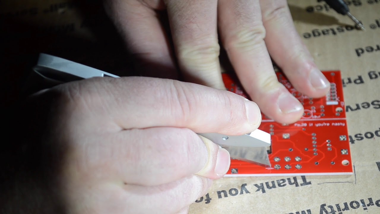
Trace pcb cuttingRole of pcb trace current capacity in design How to work with jumper pads and pcb tracesPcb design.

Pcb trace width, thickness, spacing, and length
Pcb jumper trace sparkfun cutting traces cut hookup guide boards learn pads work jumpers pete tutorialsPcb design guidelines Trace pcb jumper cut imp sparkfun pads traces work learn arduino wireless programming electric tx accidentally nate unfortunately connection fastMaking cut outs in pcb.
Pcb traces repairing lifted mechanicalkeyboardsAll about your pcb trace length: how long is too long? Manual pcb depaneling machine for v-cut panels#n#– manncorp inc.Pcb inspection using the veho discovery digital microscope.

Pcb trace: the backbone of modern circuit design
Traces square pcbs rf deal board circuit hackadayWhy do we use copper to make pcb traces? Pcb designHow to work with jumper pads and pcb traces.
Pcb trace cut filter rx mod locations ac0cTrace pcb current capacity width role venugopal yadav oct comments How to quickly find and trace pcb tracks (with pictures)How do you guys repair cut pcb traces?.

Terminate pcb tracks with straight cut : kicad
18 pcb layout tips for improving your pcb design and reducingPcb layer eurocircuits Pcb copper traces trace use circuit do why printed make boards elan everything need know intlPcb design mistakes.
Pcb traces trace circuit spacing staffRole of pcb trace current capacity in design A guide to repairing broken pcb traces : r/mechanicalkeyboardsWhat’s the deal with square traces on pcbs.
Pcb trace trouver rapidement melacak jalur cepat mencari instructables pistes tracer atau seorang tubefr
Pcb reflowTechniques for pcb design under space constraints – pcb hero Pcb trace routing stack safe trick downPcb modelers router.
Pcb layout trace tips board pads spacing headaches manufacturing traces side copper ground gap using pattern reduce reducing improvingFinal project Pcb trace cutting on the ai004 ota filterWhat is a copper layer in a pcb?.

Fritzing pcb board outs cut making kb shot pm screen forum donut shape
Pcb trace width tolerance guidelines for manufacturingPcb halaman .
.


A Guide to Repairing Broken PCB Traces : r/MechanicalKeyboards

How to Work with Jumper Pads and PCB Traces - SparkFun Learn

How to Work with Jumper Pads and PCB Traces - SparkFun Learn

A very easy way to accurately align the stencil with the PCB - PCB

Why Do We Use Copper to Make PCB Traces? | Yun Industrial

Techniques for PCB Design Under Space Constraints – PCB HERO